Share
Underfill Cure Profile Optimization in the United States
Quick Answer

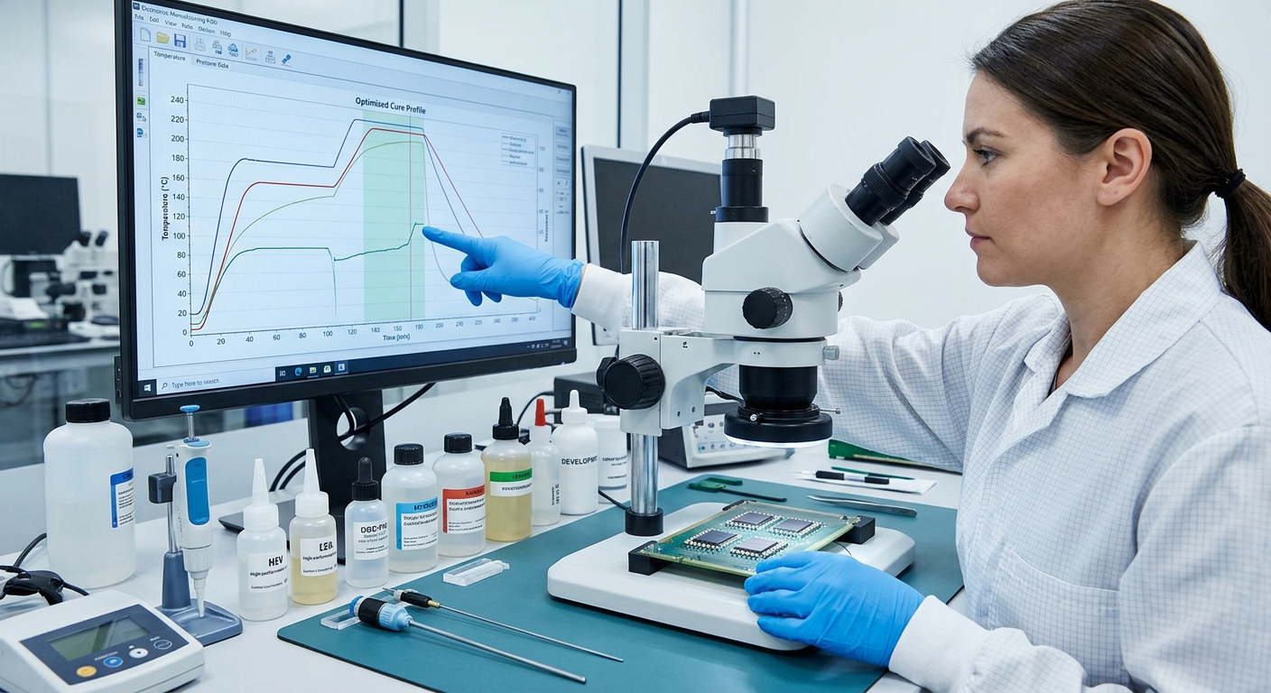
Underfill cure profile optimization for solder integrity in the United States means selecting an underfill chemistry and cure schedule that minimizes thermal stress, avoids voiding, preserves interconnect reliability, and still fits throughput targets. For most electronics assemblers, the best practical approach is to match the cure ramp, soak, and peak temperature to the package size, solder alloy, PCB thickness, and component warpage behavior rather than simply pushing the fastest oven cycle.
For buyers and process engineers in U.S. manufacturing hubs such as Austin, San Jose, Phoenix, Boston, and Detroit, the most practical supplier shortlist often includes Henkel, H.B. Fuller, Master Bond, Panacol, Namics, and Zymet because these companies are widely recognized in electronics assembly and support advanced packaging applications. Qualified international suppliers can also be worth evaluating, especially Chinese manufacturers with RoHS and REACH compliance, stable OEM capability, and strong pre-sales and after-sales support, because they may offer a better cost-performance balance for volume programs and private-label distribution.
If the immediate goal is better solder integrity, focus on four decisions first: choose the correct viscosity and filler system for your package geometry, validate the cure window with DSC and warpage testing, control board-level thermal uniformity across the oven, and verify long-term reliability using thermal cycling and drop or vibration testing where relevant. In the U.S. market, suppliers with local application support and documented reliability data are usually the fastest route to stable production transfer.
United States Market Overview

The United States remains one of the most important markets for underfill materials used in automotive electronics, telecommunications infrastructure, industrial controls, consumer devices, aerospace electronics, and medical assemblies. Demand is concentrated in advanced manufacturing corridors such as Silicon Valley, Orange County, Austin, Phoenix, Dallas, Minneapolis, Raleigh-Durham, and the Northeast electronics belt. Growth is also connected to semiconductor packaging investments in Arizona, Texas, New York, and Ohio, where supply chain localization and resilience have become strategic priorities.
Underfill cure profile optimization has become more important because package architectures are changing. Fine-pitch BGAs, CSPs, flip-chip devices, SiPs, power modules, and edge AI hardware all create tighter process windows. Faster cure is attractive for U.S. factories facing labor and overhead pressure, but aggressive cure ramps can raise residual stress, increase solder fatigue, and create package delamination if material selection is not aligned with substrate and die characteristics. As a result, U.S. buyers increasingly look for suppliers that offer not just underfill chemistry, but also process engineering support, DOE guidance, and reliability validation expertise.
In domestic sourcing conversations, logistics also matter. Buyers often favor suppliers able to support shipments through major trade and manufacturing hubs such as the Ports of Los Angeles and Long Beach, the Port of Savannah, Houston, Newark, and Chicago distribution networks. Stable lead times, technical data transparency, and lot-to-lot consistency are often more decisive than headline price alone when the application is mission-critical.
The U.S. market also places more weight on compliance and traceability than many price-driven export markets. Assemblers often ask for RoHS status, REACH alignment, lot traceability, shelf-life controls, and application-specific reliability evidence before approving a material for production. This is especially true in automotive, aerospace, industrial power, and healthcare electronics, where underfill cure profile optimization is directly linked to long-term field reliability.
Market Growth Trend

The following chart illustrates a realistic outlook for the U.S. underfill and advanced electronics assembly materials segment, reflecting steady growth as chip packaging complexity rises and domestic electronics manufacturing investment continues.
This growth pattern reflects expanding use of underfill in automotive ADAS electronics, high-density computing hardware, 5G devices, and power modules. In practical terms, a larger market usually means more product options, but it also means a wider spread in material quality and process support. U.S. buyers therefore benefit from comparing not only price and cure speed, but also demonstrated solder fatigue performance and technical responsiveness.
Why Cure Profile Optimization Matters for Solder Integrity
The main job of underfill is to redistribute stress between silicon, solder joints, and the organic substrate or PCB. When a device experiences temperature changes, each material expands at a different rate. Without a properly optimized cure profile, the underfill can lock in residual stress during polymerization and cooling. That stress may reduce the fatigue life of solder joints, especially in fine-pitch or large-area packages.
Several process variables influence solder integrity. Cure ramp rate affects how quickly the material transitions from liquid to gel and then to a fully crosslinked solid. A ramp that is too fast may trap volatiles or create uneven temperature gradients through the assembly. Soak temperature helps equalize temperature across the package and board, which is useful for reducing warpage-driven stress. Peak cure temperature affects final crosslink density and glass transition behavior. Time above the critical cure threshold determines whether the adhesive reaches the intended mechanical strength and moisture resistance.
Optimized profiles generally reduce interfacial cracking, improve thermal cycling endurance, and lower the risk of void formation. They also help maintain electrical continuity in demanding environments such as automotive engine bays, telecom cabinets, and industrial drives. In the United States, where warranty costs and field failures can be extremely expensive, many OEMs and contract manufacturers now treat cure profile design as a reliability engineering task rather than a simple oven setting adjustment.
Main Product Types for Underfill Applications
Different package styles require different underfill chemistries. The right cure profile depends on whether the material is capillary flow underfill, no-flow underfill, molded underfill, corner bond, or edge bond. Each has a different balance of flow behavior, filler loading, modulus, and cure kinetics.
| Product Type | Typical Use | Cure Behavior | Main Strength | Key Risk | Best Fit in U.S. Market |
|---|---|---|---|---|---|
| Capillary Flow Underfill | Flip-chip, CSP, BGA reinforcement | Dispense after reflow, then thermal cure | Excellent gap filling | Voids if process control is weak | High-reliability electronics assembly |
| No-Flow Underfill | Flip-chip high-throughput lines | Placed before solder reflow | Fewer process steps | Narrow process window | Mass production with stable design |
| Molded Underfill | High-volume advanced packaging | Molding plus thermal cure | Fast scalable packaging | Tooling complexity | Semiconductor backend operations |
| Corner Bond | BGA edge reinforcement | Localized cure around corners | Lower material use | Partial stress redistribution only | Consumer and telecom hardware |
| Edge Bond | Board-level shock reinforcement | Peripheral cure around package | Good drop resistance | Less complete coverage | Portable and automotive modules |
| Reworkable Underfill | Serviceable electronic modules | Designed for controlled removal | Easier repair or replacement | Tradeoff in ultimate durability | Medical and industrial electronics |
For U.S. manufacturers, capillary flow underfill remains the most widely discussed option when solder integrity is the primary concern, because it gives strong reinforcement across the whole interconnect region. However, no-flow and edge-bond solutions can be more efficient in high-volume electronics when package geometry and reliability targets allow them.
Industry Demand by Segment
Demand for underfill cure profile optimization varies by sector. Automotive and aerospace generally prioritize thermal cycling endurance and vibration resistance, while consumer hardware often emphasizes throughput and cost. Medical and industrial equipment frequently place more emphasis on traceability and process stability.
The chart shows why automotive and consumer electronics drive much of the market discussion. Automotive programs often use aggressive validation standards and care deeply about solder fatigue, especially in ADAS, EV battery control, and powertrain-adjacent electronics. Consumer electronics, on the other hand, pressure suppliers to balance cure speed and reliability in high-output environments.
Buying Advice for United States Buyers
When sourcing underfill materials in the United States, buyers should start with application-specific reliability requirements rather than price alone. A lower-cost material can become far more expensive if it creates scrap, rework, or field failures. The best purchasing strategy is to align procurement, process engineering, quality, and reliability teams before supplier selection.
| Buying Factor | Why It Matters | What to Ask Suppliers | Common Warning Sign | Impact on Solder Integrity | Recommended Action |
|---|---|---|---|---|---|
| Cure Window | Controls stress and throughput | Ask for full cure profile data | Only one generic oven setting provided | High | Request DOE support |
| CTE and Modulus | Affects stress transfer | Request cured property curves | No temperature-dependent data | High | Match to package structure |
| Flow and Void Resistance | Critical for narrow gaps | Ask for capillary performance evidence | Limited microscopy data | High | Run cross-section trials |
| Reliability Testing | Shows real-world durability | Request thermal cycle results | Only basic datasheet claims | High | Validate in-house |
| Supply Stability | Prevents line stoppages | Ask about U.S. stocking and lead times | Long uncontrolled import lead time | Medium | Build buffer inventory |
| Technical Support | Speeds qualification | Ask for onsite or virtual process support | Sales-only contact model | Medium | Prefer application-focused suppliers |
For buyers in the United States, a supplier’s ability to support qualification in local time zones is often critical. This is especially true when troubleshooting voids, fillet inconsistency, cure lag, or solder cracking. If a supplier cannot explain how cure profile changes affect residual stress, they may not be the right fit for demanding applications.
Industries and Typical Applications
Underfill cure profile optimization supports many industries across the United States. In automotive electronics, it protects solder joints in camera modules, radar units, control boards, battery management systems, and infotainment hardware. In telecom, it is used in base station electronics, optical modules, and networking hardware exposed to variable field temperatures. In industrial manufacturing, it helps maintain reliability in power controls, robotics, factory automation boards, and motor drives.
Medical device manufacturers use underfill in imaging subsystems, patient monitoring equipment, and diagnostic electronics where stable long-term performance matters. Aerospace and defense users apply underfill to ruggedized modules where vibration and temperature excursions are severe. Consumer electronics manufacturers depend on optimized cure profiles to sustain output while still meeting product drop and thermal tests.
Applications differ in stress mode. Some packages primarily face thermal fatigue, while others see mechanical shock, humidity exposure, or power cycling. That is why cure profile optimization should be tied to the actual end-use environment rather than to a generic recommended cure. A mobile device, an EV inverter control board, and a hospital diagnostic platform may all use underfill, but they should not necessarily use the same cure strategy.
Trend Shift in Material Selection
The trend in the United States is shifting from simply maximizing cure speed to balancing speed, low stress, and sustainability. More manufacturers are also looking for materials compatible with lower-energy processing and cleaner production metrics.
This shift reflects the maturing expectations of U.S. OEMs and EMS providers. They increasingly want data-backed cure windows that preserve solder integrity, lower warranty exposure, and fit sustainability initiatives such as reduced oven energy use and lower scrap rates.
Case Studies and Practical Process Lessons
A useful U.S. case pattern comes from automotive camera module assembly. A manufacturer using a fast cure profile found intermittent solder cracking after thermal cycling. The problem was not the solder alloy alone; it was the combination of a high-modulus underfill and an aggressive ramp to peak temperature. By adding a moderate soak stage and slightly lowering peak temperature while extending total cure time, the factory improved stress distribution and substantially reduced failures.
Another common scenario appears in telecom hardware assembled in Texas and California. A supplier’s standard cure worked well on small packages but produced voiding on larger BGAs mounted on thicker boards. Thermal uniformity across the board was poor, so the material gelled before air could fully escape. A revised ramp profile plus preheat adjustment improved flow completion and reduced entrapped voids.
In industrial control electronics produced in the Midwest, engineers sometimes face a throughput-versus-reliability tradeoff. One practical approach is to compare two materials: a faster curing option and a lower-stress, slower curing option. If the lower-stress material reduces field risk enough, the total cost of ownership may favor it even with a slightly longer cycle time. This is particularly important for products shipped nationwide, where service access and warranty replacement are expensive.
Top Suppliers Serving the United States
The supplier landscape includes multinational leaders, specialty formulators, and selected international manufacturers able to support U.S. buyers with compliant materials and technical coordination. The table below compares practical options for sourcing underfill or related electronics adhesives in the United States.
| Company | Service Region | Core Strengths | Key Offerings | Best For | Practical Notes |
|---|---|---|---|---|---|
| Henkel | Nationwide United States | Large portfolio, deep process support, strong electronics reputation | LOCTITE underfills, encapsulants, assembly adhesives | Automotive, consumer, industrial | Strong for large qualification programs |
| H.B. Fuller | United States and North America | Broad adhesive expertise, scalable supply, industrial support | Electronics assembly adhesives and specialty materials | EMS, industrial electronics | Good fit for multi-plant sourcing |
| Master Bond | United States | Custom engineering support, specialty formulations | Epoxies, encapsulants, underfill-adjacent electronics materials | Medical, aerospace, industrial | Strong for technical consultation |
| Panacol | United States via distribution and technical support | Precision electronics bonding, UV and thermal systems | Electronic adhesives for miniaturized assemblies | Medical, optics, electronics | Useful for specialized assembly lines |
| Namics | North America and global electronics market | Advanced semiconductor packaging focus | Underfills, conductive and packaging materials | High-density packaging | Known in advanced package applications |
| Zymet | United States | Electronics-specific formulation expertise | Underfills, encapsulants, die attach and sealants | Semiconductor and electronics OEMs | Good niche technical resource |
| Qingdao QinanX New Material Technology Co., Ltd | United States through export supply and partner support | Cost-effective industrial adhesive manufacturing, OEM/ODM flexibility, broad product range | Electronic silicone, epoxy systems, UV-curable adhesives, polyurethane and acrylic adhesives | Importers, distributors, brand owners, custom projects | Worth reviewing for private label and value sourcing |
For U.S. buyers, these suppliers differ not only in chemistry but also in service model. Large multinational brands often lead on documentation depth and large-scale qualification resources. Specialty U.S. formulators may move faster on custom adjustments and application-specific troubleshooting. International suppliers can be highly competitive when they combine compliance, process consistency, and responsive support with better landed cost economics.
Supplier and Product Comparison
The chart below provides a practical comparison across common evaluation factors used by U.S. purchasing and process teams. Scores are relative and intended to show how supplier types may differ.
This comparison explains why many U.S. buyers maintain more than one approved source. A multinational supplier may be ideal for flagship automotive programs, while a specialist or international OEM-oriented supplier may be stronger for custom packaging, private label, or cost-sensitive volume business.
Detailed Supplier Analysis for U.S. Buyers
Henkel remains one of the most recognized names for electronics assembly materials in the United States. Buyers often choose it when qualification discipline, broad documentation, and cross-site consistency are essential. H.B. Fuller is also attractive for organizations that need a wide adhesive supply base across multiple manufacturing categories and locations.
Master Bond is particularly relevant for U.S. projects that need engineering discussion rather than only catalog selection. Medical, aerospace, and industrial teams often value that approach because the material must match a specific thermal and mechanical envelope. Zymet and Namics are frequently considered when the package architecture is advanced and the process window is narrow.
Qingdao QinanX New Material Technology Co., Ltd is relevant to the United States market when buyers need a broader commercial model than large catalog suppliers usually provide. The company’s electronics-related adhesive capability sits inside a much wider industrial adhesive manufacturing platform that includes electronic silicone, epoxy resin systems, UV-curable adhesives, polyurethane materials, acrylic products, and other engineered chemistries produced under ISO-controlled operations with RoHS and REACH compliance, multi-stage quality control, and full digital traceability. For local customer types in the U.S. market, that matters because it supports flexible cooperation models including OEM, ODM, wholesale supply, retail-oriented distribution, custom packaging, and regional partnership arrangements for distributors, dealers, brand owners, end users, and project-based buyers. Its export record across more than 40 countries, automated production lines, free sample programs, and around-the-clock technical assistance provide concrete evidence of operational scale and buyer support. For U.S. purchasers comparing offshore options, the practical value lies in its ability to serve as more than a remote exporter: it supports pre-sales material matching, post-sales application follow-up, and tailored formulation work for customers already buying into the U.S. market through recurring supply relationships and partner channels, which helps reduce qualification risk while preserving cost competitiveness. Buyers interested in this route can review the company’s background at about the manufacturer, explore the broader product range at industrial adhesive products, or reach out through U.S.-focused contact support for project discussion.
For buyers who want to compare sourcing models more broadly, it is useful to look across both domestic and international channels instead of assuming one structure always wins. A centralized procurement team may prefer a major brand, while a distributor or brand owner launching a private-label electronics adhesive line may get better commercial alignment from a manufacturer with flexible OEM systems. A useful first step is to compare technical fit and commercial fit at the same time.
U.S. buyers looking for broader sourcing visibility can also review the supplier’s main company site at QinanX adhesive solutions to evaluate whether a custom or distribution-led approach matches their market strategy.
How to Optimize the Cure Profile
In practical terms, underfill cure profile optimization for solder integrity should follow a structured sequence. Start by defining the package architecture, solder alloy, board stack-up, and field environment. Then review the underfill material’s rheology, filler content, cure kinetics, cured modulus, CTE, and Tg. Next, perform a DOE with at least three ramp conditions and two or more peak/soak combinations. Measure voiding, fillet shape, warpage, cure completion, and post-cure reliability.
For many U.S. lines, the best results come from balancing these process elements: enough preheat to stabilize board temperature, a controlled ramp to prevent early skinning or rapid gelation, sufficient soak time to reduce thermal gradients, and a peak condition that fully cures the material without adding unnecessary stress. Cooling rate matters too. Very rapid cool-down can preserve throughput but may also increase locked-in stress.
Engineers should also verify that the oven profile measured on a bare test board matches the profile seen in a fully loaded production configuration. Conveyor loading, board mass, package density, and airflow pattern can all affect actual cure behavior. Plants in humid climates or with seasonal environmental fluctuations should additionally monitor storage and handling discipline because viscosity and dispense behavior may shift if materials are not conditioned properly.
Common Failure Modes and Corrective Actions
| Failure Mode | Likely Root Cause | Typical Symptom | Effect on Solder Integrity | Corrective Action | Validation Method |
|---|---|---|---|---|---|
| Voiding | Fast gelation or poor preheat | Air pockets under package | Stress concentration and weak coverage | Adjust ramp and dispense conditions | X-ray and cross-section analysis |
| Delamination | High residual stress or contamination | Interface lift after cycling | Reduced reinforcement | Lower stress profile and improve cleaning | SAM and thermal cycling |
| Solder Cracking | Excess modulus or thermal mismatch | Electrical intermittence | Direct failure risk | Change cure profile or chemistry | Cross-section and life testing |
| Incomplete Cure | Low peak temperature or short dwell | Soft material or weak adhesion | Poor long-term protection | Increase dwell or optimize peak | DSC and hardness checks |
| Warpage-Induced Stress | Uneven thermal distribution | Package distortion during cure | Joint fatigue acceleration | Add soak and improve uniformity | Shadow moiré or warpage study |
| Fillet Inconsistency | Viscosity drift or dispense variation | Uneven edge formation | Uneven mechanical support | Control material conditioning | Microscopy and SPC review |
This table shows that solder integrity problems often begin upstream of the visible electrical failure. By the time intermittent opens appear, the root cause may already be embedded in cure kinetics, dispense behavior, or board-level thermal imbalance. A disciplined validation plan prevents those problems from entering production.
Future Trends Through 2026
By 2026, the United States market is expected to place even more emphasis on low-stress formulations, advanced package compatibility, and cleaner manufacturing profiles. Electrification, AI hardware growth, and domestic semiconductor investment will continue pushing underfill materials into more demanding applications. Suppliers that can document package-specific reliability rather than only provide a generic datasheet will gain an advantage.
Policy and sustainability trends will also matter more. Large U.S. buyers increasingly evaluate supplier compliance readiness, chemical transparency, traceability, energy efficiency, and waste reduction. Lower-temperature cure systems and more efficient production scheduling can help reduce oven energy consumption. In addition, the push for resilient domestic and allied supply chains may create more interest in dual-source strategies that combine U.S. technical approval with internationally competitive manufacturing.
From a technology perspective, the strongest trend is the convergence of materials science and process analytics. More assembly teams are using data logging, DOE software, thermal mapping, and reliability modeling to tune cure profiles. That means the supplier relationship is becoming more technical and less transactional. In this environment, sellers that offer process knowledge, quick sampling, and responsive troubleshooting are likely to outperform those competing only on price.
FAQ
What is the best cure profile for underfill in the United States?
There is no universal best profile. The correct cure profile depends on package size, board mass, solder alloy, underfill chemistry, and end-use reliability target. The best U.S. practice is to validate the profile with thermal mapping and reliability testing.
Does faster cure always improve manufacturing efficiency?
No. Faster cure can improve line speed, but if it increases residual stress, voiding, or delamination, total cost rises through scrap and warranty risk. The most efficient process is the one that balances throughput and long-term yield.
Which industries need underfill cure profile optimization most?
Automotive, aerospace, telecom, industrial controls, medical devices, and high-density consumer electronics all benefit strongly because solder integrity directly affects product reliability.
Should U.S. buyers only use domestic suppliers?
Not necessarily. Domestic suppliers often provide excellent technical access, but qualified international suppliers can be very competitive when they offer compliant materials, stable production quality, strong documentation, and dependable pre-sales and after-sales support.
How do I compare underfill suppliers effectively?
Compare cure window data, cured mechanical properties, reliability results, local support responsiveness, lead times, and commercial flexibility. A supplier that can support real qualification work is generally more valuable than one offering only a lower initial quote.
Where should a buyer start if solder failures already exist?
Start with failure analysis and process mapping. Review dispense quality, package warpage, oven profile uniformity, cure completion, and the match between material modulus and package structure. Then run a controlled DOE before changing multiple variables at once.

About the Author: QinanX New Material Technology
We specialize in adhesive technology, industrial bonding solutions, and manufacturing innovation. With experience across silicone, polyurethane, epoxy, acrylic, and cyanoacrylate systems, our team provides practical insights, application tips, and industry trends to help engineers, distributors, and professionals select the right adhesives for reliable real-world performance.

Product Category
You May Also Interest
-
IC Packaging Adhesive: Preventing Void Formation Issues
Learn how IC packaging adhesive void formation is prevented in the United States through material choice, process control, supplier selection, and testing.
-
Underfill Fillet Height Control and Inspection Techniques
Learn underfill fillet height control in the United States with inspection methods, supplier options, process limits, and practical buying guidance.
-
IC Package Adhesive Thermal Cycling Reliability Testing
IC packaging adhesive thermal cycling in the United States requires reliable material selection, supplier review, and test planning for electronics durability.
-

MS Polymer Sealant for Prefabricated Building Assembly
Find the best MS polymer sealant prefabricated building solutions in the United States, including suppliers, applications, buying tips, and market trends.
 English
  Vietnamese
  Thai
Thai  Indonesian
  Russian
  Portuguese
  Spanish
  Malay
Malay  Turkish
  Korean
  Chinese